Surface mount technology has revolutionized how you interact with modern electronics. It allows manufacturers to produce smaller, faster, and more efficient devices, meeting the growing demand for high-performance gadgets. For instance:
-
High-speed SMT lines represented 46.66% of the market share in 2023, valued at $2,707.03 million, and are expected to grow at a CAGR of 8.50%.
-
Consumer electronics, a major driver, held 35.88% of the SMT market, valued at $2,081.46 million, with a projected CAGR of 8.94%.
The significance of PCB assembly lies in its ability to support industries like automotive, IoT, and telecommunications. By ensuring precise component placement and soldering, this process enhances the quality and reliability of every electronic device you use.
Key Takeaways
-
SMT helps make smaller, faster, and better electronic devices.
-
Solder paste is key for strong joints; good stencils help.
-
Pick-and-place machines quickly and accurately put parts in place.
-
Reflow soldering connects parts; heat control stops mistakes.
-
After assembly, checks and tests ensure PCBs work well.
-
Following IPC rules keeps PCB quality steady and reliable.
-
AI tools find problems early, improving quality control.
-
Using data and training workers makes assembly better over time.
Key Processes in the PCB Assembly Process
Solder Paste Application
Stencil printing and its role in precision
Solder paste printing is the first step in the PCB assembly process. You use a stencil to apply solder paste onto the circuit board's pads, ensuring precise deposits for strong solder joints. Proper stencil design is critical for achieving accuracy. For example:
-
Opening Separation: Clean paste deposits prevent solder bridging.
-
Stencil Thickness Selection: Thinner stencils work best for fine-pitch components, while thicker stencils suit larger ones.
-
Step Stencils: These optimize solder volume distribution for PCBs with mixed component sizes.
Fiducial marks play a vital role in aligning the stencil with the PCB. Using durable materials like stainless steel or nickel ensures long-lasting precision during solder paste printing.
Solder paste inspection (SPI) for quality control
After solder paste printing, you inspect the application using SPI tools. These systems detect defects such as insufficient paste volume or misaligned deposits. SPI ensures that the soldering process proceeds without issues, reducing the risk of faulty connections.
Key Process | Importance |
|---|---|
Solder Paste Application | Ensures effective solder connections during reflow, critical for the functionality of the PCB. |
Component Placement
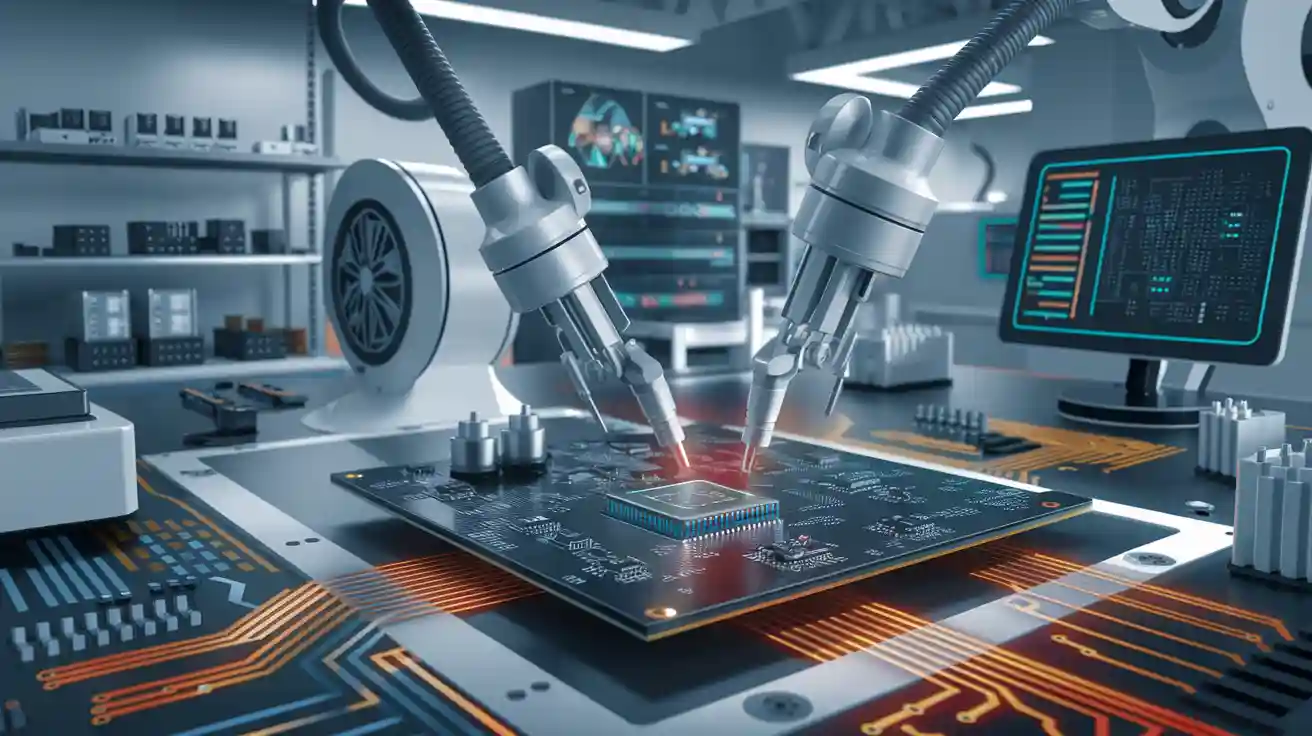
Automated pick-and-place machines
Automated pick-and-place machines streamline the circuit card assembly process. These machines use CAD files and pick-and-place files to position components accurately on the PCB. High-speed operation and precision make them indispensable for modern PCB assembly.
Ensuring accuracy in component alignment
Alignment accuracy is crucial for the functionality of the final product. You can achieve this by employing best practices such as:
-
Inspecting components for damage before assembly.
-
Using solder paste inspection to verify application quality.
-
Leveraging AOI systems to detect misalignments after soldering.
Inspection Method | Description |
|---|---|
Ensures components meet specifications and are free of damage before assembly. | |
AOI Inspection | Uses high-resolution cameras to identify issues like misalignments and insufficient solder after soldering. |
Reflow Soldering
Importance of temperature profiling
Reflow soldering solidifies the connections between components and the PCB. Temperature profiling ensures that the soldering process achieves optimal results. You monitor the temperature curve to prevent overheating or insufficient heat, which can lead to defects.
Addressing common soldering defects
Defects like solder bridging, voids, and cold joints can compromise the quality of the PCB assembly process. You can minimize these issues by:
-
Using X-ray inspection to detect hidden solder joint problems.
-
Employing ICT to verify electrical connectivity and performance.
Reflow soldering is a critical step in circuit card assembly, as it determines the reliability of the final product.
Post-Assembly Inspection and Testing
Visual inspection for initial defect detection
Visual inspection is the first step in post-assembly testing. It helps you identify obvious defects before moving to advanced testing methods. You can use manual inspection tools to check for issues like solder bridges, cold solder joints, or open solder connections. These defects often occur during soldering and can compromise the functionality of the PCB assembly.
During visual inspection, you focus on the physical attributes of the board. You verify the dimensions, warpage, and solder joint quality. This process ensures that the board meets basic standards before undergoing electrical testing.
Tip: Use magnification tools like microscopes or magnifiers to enhance defect detection during manual inspection.
Purpose | Defects Identified | |
|---|---|---|
Manual Inspection | Verify board's warpage, dimensions, and solder joints | Solder bridges, open solder, cold solder, etc. |
Visual inspection is a cost-effective method for initial defect detection. It allows you to catch errors early, reducing the need for rework later in the process.
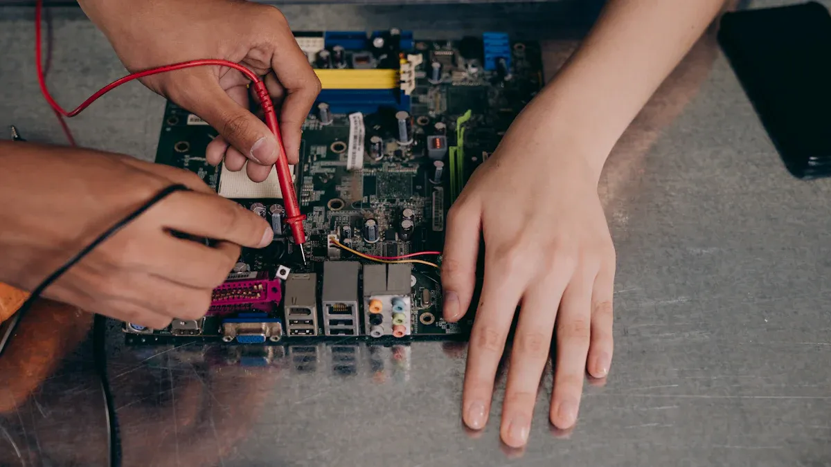
In-circuit testing (ICT) for electrical functionality
In-circuit testing (ICT) is a critical step in ensuring the electrical functionality of the PCB assembly. This method examines the electrical properties of the board, such as resistance, capacitance, and continuity. ICT helps you identify shorts, opens, and incorrect components that may have been introduced during soldering or component placement.
ICT uses specialized probes to test individual circuits on the PCB. These probes measure electrical quantities and compare them to predefined values. If a circuit fails to meet the expected parameters, you can pinpoint the issue and address it before the board moves to the next stage.
Functional testing complements ICT by verifying the overall performance of the PCB. It ensures that the board operates as intended and is ready for dispatch. Together, these testing methods provide a comprehensive evaluation of the PCB assembly's quality.
Inspection Test Type | Purpose | Defects Identified |
|---|---|---|
In-Circuit Testing | Examine electrical quantities like resistance and capacitance | Shorts, opens, incorrect components |
Functional Testing | Determine if the board is ready for dispatch | Signal integrity issues, incorrect voltage or current |
Note: Regular calibration of ICT equipment ensures accurate measurements and reliable testing results.
Post-assembly inspection and testing are essential for delivering high-quality electronic products. By combining visual inspection and ICT, you can ensure that every PCB assembly meets industry standards and performs reliably in its intended application.
Technologies in Surface Mount Technology PCB Assembly
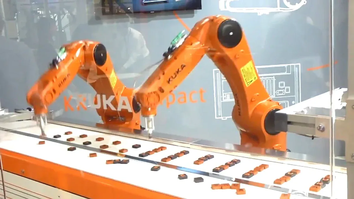
Automated Placement Machines
Features enhancing efficiency and precision
Automated placement machines are the backbone of modern PCB assembly lines. These machines bring unmatched speed and precision to the process of placing components on circuit boards. Key features that enhance their performance include:
-
Multi-head, high-speed placement systems: These systems can place tens of thousands to hundreds of thousands of components per hour, significantly boosting production rates.
-
High-precision visual recognition systems: Advanced technology ensures placement accuracy for tiny components, achieving tolerances as fine as ±25μm.
-
Intelligent feeding systems: These systems automate material identification, reducing human error and ensuring smooth operation.
-
Self-learning and predictive maintenance: AI-driven algorithms predict equipment failures, minimizing downtime and improving overall equipment efficiency (OEE).
-
Data linkage with other equipment: Integration with solder paste inspection and reflow soldering systems enables closed-loop quality control.
These features make automated component placement not only faster but also more reliable, ensuring consistent results across high-volume production runs.
Benefits of automation in high-volume production
Automation transforms the efficiency of high-volume PCB assembly. By implementing intelligent mounters, manufacturers have reported a 60% increase in output and a 30% reduction in defects. Automation also allows for rapid type changeovers, enabling you to adapt quickly to changing production demands. With fewer manual interventions, you can achieve higher per capita output while maintaining exceptional quality.
Reflow Ovens
Types of reflow ovens and their applications
Reflow ovens play a critical role in solidifying solder joints during PCB assembly. You can choose from several types of reflow ovens, each suited to specific applications:
-
Convection ovens: Ideal for general-purpose soldering, these ovens use heated air to transfer heat evenly across the PCB.
-
Vapor phase ovens: These ovens offer precise thermal control, making them suitable for high-reliability applications like aerospace and medical devices.
-
Infrared ovens: These are cost-effective options for smaller-scale production, using infrared radiation to heat the solder.
Selecting the right type of oven depends on your production needs, component types, and desired soldering quality.
Thermal control for consistent soldering quality
Maintaining consistent thermal profiles is essential for achieving high-quality solder joints. Reflow ovens equipped with advanced thermal control systems ensure uniform heating across the PCB. This minimizes defects like solder bridging or cold joints. By monitoring and adjusting the temperature curve, you can optimize the soldering process for both leaded and lead-free assemblies.
Inspection and Quality Control Tools
Automated Optical Inspection (AOI) for defect detection
Automated optical inspection (AOI) systems are indispensable for detecting defects in PCB assemblies. These systems use high-resolution cameras and advanced algorithms to identify issues like misaligned components, insufficient solder, or missing parts. AOI offers several advantages:
-
Speed: It quickly scans entire boards, making it ideal for high-volume production.
-
Non-destructive testing: AOI ensures the integrity of the PCB without causing damage.
-
Versatility: It can detect a wide range of defects, from cosmetic flaws to functional issues.
By incorporating AOI into your assembly line, you can enhance inspection and quality control while reducing the risk of defective products reaching the market.
X-ray inspection for hidden solder joint issues
X-ray inspection is a powerful tool for identifying hidden defects, such as voids or cracks in solder joints. This method is particularly useful for complex assemblies with high-density components. While X-ray systems can be costly, their ability to detect internal defects makes them invaluable for ensuring the reliability of critical applications.
Inspection Method | Advantages | Limitations |
|---|---|---|
Manual Inspection | Relies on human expertise for defect detection. | Limited by human error and fatigue. |
Automated Optical Inspection (AOI) | Fast detection of various defects, non-destructive. | Can be expensive and complex. |
X-ray Imaging | Effective for internal defects. | High cost and time-consuming. |
Combining AOI and X-ray inspection provides a comprehensive approach to maintaining high standards in surface mount technology PCB assembly.
Emerging Innovations in SMT Technologies
AI-driven defect detection systems
Artificial intelligence (AI) is transforming how you approach quality control in surface mount technology. AI-driven defect detection systems analyze real-time data to identify issues during the assembly process. These systems use machine learning algorithms to recognize patterns and predict potential defects before they occur. This proactive approach reduces downtime and enhances production efficiency.
For example, AI-powered inspection systems can detect soldering defects, misaligned components, or missing parts with remarkable accuracy. Unlike traditional methods, these systems continuously improve by learning from data patterns. This means you can achieve faster inspections and higher defect detection rates, ensuring consistent quality in your PCB assemblies.
AI also plays a critical role in predictive maintenance. By monitoring equipment performance, it identifies signs of wear or malfunction early. This allows you to schedule maintenance before a breakdown occurs, minimizing disruptions and extending the lifespan of your machinery.
Innovation Type | Description |
|---|---|
Enhances quality control and production efficiency by analyzing real-time data and predicting defects early. | |
AI in Inspection Systems | Improves defect detection accuracy and speed, learning from data patterns to enhance inspection processes. |
The integration of AI into SMT processes not only improves defect detection but also optimizes overall production workflows.
Advancements in miniaturization and high-density PCBs
The demand for smaller, more powerful electronic devices drives advancements in miniaturization and high-density PCBs. You see this trend in smartphones, wearables, and IoT devices, where space constraints require innovative solutions.
Advances in materials science have enabled the development of smaller electronic components. These components maintain high performance while occupying less space on the PCB. For instance, resistors, capacitors, and ICs are now available in ultra-miniature sizes, making it possible to design compact yet powerful devices.
High-density interconnect (HDI) technology is another game-changer. It allows you to create PCBs with more layers and finer traces, maximizing the use of available space. This is essential for applications like 5G devices and advanced medical equipment, where performance and reliability are paramount.
Innovation Type | Description |
|---|---|
Miniaturized Components | Advances in materials science enable the development of smaller electronic components, essential for modern electronics. |
Miniaturization and HDI technology push the boundaries of what you can achieve with surface mount technology. They allow you to meet the growing demand for compact, high-performance electronics while maintaining reliability and efficiency.
Tip: When designing for miniaturization, ensure your PCB layout accounts for thermal management and signal integrity to avoid performance issues.
Quality Control Measures in SMT PCB Assembly
Industry Standards and Compliance
IPC standards for PCB assembly quality
Adhering to IPC standards ensures that your PCB assembly meets globally recognized benchmarks for quality and reliability. These standards define the criteria for soldering, component placement, and overall assembly processes. By following IPC guidelines, you can achieve consistent results and reduce the risk of defects. For example, IPC-A-610 specifies the acceptability of electronic assemblies, while IPC-J-STD-001 focuses on soldering materials and techniques.
IPC standards also promote environmental sustainability in electronics. They simplify compliance management and make it easier to communicate adherence to regulations. This is particularly important as the industry continues to evolve with advancements like microvias and flex-PCBs, which require stringent quality assurance measures.
Adherence to RoHS and environmental regulations
Compliance with RoHS (Restriction of Hazardous Substances) regulations is essential for ensuring the safety and environmental responsibility of your PCB assembly processes. These regulations prohibit the use of hazardous substances like lead and mercury, making your products safer for both users and the environment.
RoHS and REACH guidelines also emphasize the elimination of toxic substances, enhancing product safety and reducing environmental impact. By adhering to these regulations, you not only meet legal requirements but also contribute to a more sustainable electronics industry. For instance, nova's pcba services collaborate with top-tier factories and engineers from Fortune 500 companies to ensure compliance and maintain high-quality standards.
Inspection and Quality Control Techniques
Best practices in visual inspection
Visual inspection remains a cornerstone of quality control in PCB assembly. It allows you to identify visible defects such as soldering irregularities, misaligned components, and surface anomalies. To enhance the effectiveness of this process, you can use magnification tools like microscopes or magnifiers.
Incorporating best practices ensures thorough inspections. For example:
-
Train operators to recognize common defects.
-
Use standardized checklists to maintain consistency.
-
Implement ergonomic workstations to reduce operator fatigue.
Visual inspection guarantees that your PCB assemblies meet basic quality standards before moving to advanced testing methods.
Purpose | Outcome | |
|---|---|---|
Visual Inspection | Identify visible defects, surface irregularities, and anomalies | Ensures overall quality and functionality of parts |
Functional testing for performance assurance
Functional testing evaluates the performance of your PCB assemblies under simulated operating conditions. This step verifies that the board meets the required performance standards and operates reliably in real-world applications.
During functional testing, you assess parameters like signal integrity, voltage levels, and current flow. This process complements visual inspection by focusing on the electrical functionality of the assembly. Together, these techniques form a comprehensive approach to quality assurance.
Inspection Technique | Purpose | Outcome |
|---|---|---|
Functional Testing | Evaluate performance under simulated operating conditions | Verifies parts meet required performance standards in real-world use |
Error Prevention and Process Optimization
Design for Manufacturability (DFM) principles
Design for Manufacturability (DFM) principles play a crucial role in preventing errors during PCB assembly. By optimizing your design for the manufacturing process, you can minimize the risk of defects and improve overall efficiency. Key DFM strategies include:
-
Simplifying the PCB layout to reduce complexity.
-
Ensuring proper spacing between components to avoid soldering issues.
-
Selecting materials that are compatible with your assembly processes.
Implementing DFM principles not only enhances quality but also reduces production costs and lead times.
Real-time process monitoring and feedback systems
Real-time process monitoring allows you to identify and address issues as they occur. By using advanced sensors and data analytics, you can track key parameters like soldering temperature, component placement accuracy, and inspection results.
Feedback systems provide actionable insights, enabling you to make immediate adjustments to your assembly line. This proactive approach minimizes downtime and ensures consistent quality. For example, integrating real-time monitoring with automated optical inspection (AOI) systems creates a closed-loop process control system.
Description | |
|---|---|
Solder Paste Inspection (SPI) | Ensures correct application of solder paste to prevent defects. |
Automated Optical Inspection (AOI) | Detects visual defects on PCBs during assembly. |
X-ray Inspection | Allows for internal inspection of solder joints and components. |
Functional Circuit Testing (FCT) | Tests the functionality of the assembled PCB. |
In-Circuit Testing (ICT) | Checks for electrical performance and component placement. |
By adopting these process control measures, you can maintain high standards in your PCB assembly operations.
Tip: Regularly update your process control measures to align with the latest industry standards and technological advancements.
Continuous Improvement Strategies
Leveraging data analytics for process enhancement
Data analytics plays a vital role in improving PCB assembly processes. By analyzing production data, you can identify inefficiencies and implement targeted solutions. For example, monitoring solder paste application rates or component placement accuracy helps you pinpoint areas needing adjustment. This approach ensures consistent results and enhances overall quality.
You can adopt a structured method to implement continuous improvement strategies effectively:
-
Plan: Identify a specific problem or opportunity for improvement.
-
Do: Test changes on a small scale to evaluate their effectiveness.
-
Check: Monitor results and collect data to assess the impact of the changes.
-
Act: Analyze the data and decide on the next steps, such as scaling successful changes or refining the process further.
An illustrative case highlights the redesign of a control room in a chemical plant. Ergonomic chairs and adjustable monitors reduced operator fatigue, leading to increased vigilance and faster response times.
By leveraging data analytics, you can make informed decisions that optimize your assembly line and ensure high-quality outcomes.
Training programs for operator skill development
Operator training is essential for maintaining efficiency and reducing errors in PCB assembly. Skilled operators can identify defects early, operate equipment effectively, and adapt to new technologies. Training programs should focus on both technical skills and process understanding.
You can design effective training programs by incorporating the following elements:
-
Hands-on practice: Allow operators to work with real equipment to build confidence and familiarity.
-
Regular updates: Provide ongoing training to keep operators informed about new technologies and industry standards.
-
Ergonomic considerations: Create comfortable workstations to reduce fatigue and improve focus.
Training programs that prioritize ergonomics have shown measurable benefits. For instance, adjustable monitors and ergonomic chairs enhance operator comfort, leading to better performance and fewer errors.
Investing in operator training not only improves individual performance but also strengthens the overall assembly process. Skilled operators contribute to higher productivity and ensure consistent quality in PCB assemblies.
Surface mount technology has transformed how you approach pcb assembly, enabling the creation of compact, high-performance devices. From precise solder paste application to advanced inspection tools, every step in the process ensures reliability and efficiency. Automation and innovations like AI-driven defect detection have further enhanced production quality, meeting the growing demand for smaller, faster electronics.
The evolution of SMT reflects advancements in component miniaturization, real-time analytics, and material science. For instance, new solder compounds now improve thermal properties, reducing failure rates in high-power applications. As market demand continues to rise, SMT remains at the forefront of modern electronics, driving innovation and shaping the future of technology.
Aspect | Evidence |
|---|---|
Component Miniaturization | SMT parts are significantly smaller than through-hole counterparts, enhancing design possibilities. |
Automation | Fully automated SMT production lines are integrating real-time analytics to optimize efficiency. |
Material Science | New solder compounds improve thermal properties, reducing failure rates in high-power applications. |
Market Demand | The demand for smaller, faster electronics is driving the evolution of SMT technology. |
By prioritizing precision and quality, you can ensure that your electronic products meet the highest standards, delivering exceptional performance and reliability.
FAQ
What is SMT PCB assembly?
SMT PCB assembly involves mounting electronic components directly onto the surface of a printed circuit board. This method allows for compact designs and high-speed production, making it ideal for modern electronics.
How does solder paste inspection improve quality?
Solder paste inspection ensures accurate application of solder paste on the PCB. It detects issues like insufficient paste or misalignment, reducing the risk of defects during the assembly process.
Why is temperature profiling important in reflow soldering?
Temperature profiling ensures that solder joints form correctly during reflow soldering. It prevents overheating or underheating, which can lead to defects like solder bridging or cold joints.
What are the benefits of automated optical inspection (AOI)?
AOI quickly detects defects like misaligned components or insufficient solder. It uses high-resolution cameras and algorithms, ensuring consistent quality in high-volume production.
How does real-time process monitoring enhance PCB assembly?
Real-time monitoring tracks key parameters like soldering temperature and component placement. It provides immediate feedback, allowing you to address issues quickly and maintain consistent quality.
What is the role of IPC standards in PCB assembly?
IPC standards define quality benchmarks for PCB assembly processes. Following these standards ensures reliable products and compliance with industry requirements.
How does miniaturization impact SMT PCB assembly?
Miniaturization allows for smaller, more powerful devices. It requires precise component placement and advanced technologies like high-density interconnects to maximize PCB space.
What is the difference between functional testing and in-circuit testing?
Functional testing evaluates the overall performance of the PCB under simulated conditions. In-circuit testing checks individual components and circuits for electrical functionality.


